

buried via differ from a blind via
When it comes to PCB design, there are a variety of techniques that can be used for creating signal traces on the surface. One of the most popular methods is to use vias, which are holes that connect layers on a multilayer printed circuit board. However, there are several different types of vias, including blind and buried vias. Both serve a similar purpose, but they are different in how they are created and used on the circuit board.
In this article, we’ll discuss the difference between these two vias, and what impact they can have on your next PCB project. We’ll also discuss what types of vias are best suited for which applications. Finally, we’ll discuss some considerations that you should keep in mind when designing a PCB using either of these via types.
A buried via is a type of via that exists within the internal layers of the PCB. These vias are not visible from the outside of the board, which is why they are referred to as “buried.” Buried vias can be used to connect internal layers of the PCB, or they can be used to connect signal traces present on different layers of the circuit board.
The main difference between a buried via and a blind via is that a blind via can only be seen from one side of the circuit board, while a buried via can be seen on both sides. Additionally, a buried via can be connected to multiple inner layers of the PCB, while a blind via can only be connected to one.
To make a blind and buried via, you first start with a sheet of glass-fibre cloth pre-(im)pregnated with uncured resin. Then, you add a sheet of copper foil to the top and bottom of the pre-preg. The entire build is then laminated together and processed like a double-sided PCB. The resulting “sandwich” is then drilled and plated.
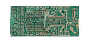
How does a buried via differ from a blind via?
Blind and buried vias are becoming more and more common on high-density circuit boards (HDI-PCB). This technology is able to maximize functionality in the same space, which can be helpful for reducing costs or improving performance.
However, using buried and blind vias requires careful consideration when designing the layer build-up of your PCB. It is important that you keep the number of blind and buried vias to a minimum in order to avoid overlapping them with other layers. In addition, it is recommended that you use staggered or stacked vias rather than straight lines whenever possible.
Both blind and buried vias can provide many benefits to your next PCB project, including increased routing density, reduced layer counts, improved impedance control, and better test access. However, there are some important considerations when using these types of vias, including how they will be fabricated, thermal management, reliability, and assembly. To ensure that you’re making the right choice, be sure to consult with an expert when designing your next PCB.
Improved Signal Integrity: Buried vias help in reducing the potential for signal degradation. In high-speed circuits, long or poorly placed vias can introduce signal loss or delay. By placing the vias within the inner layers, buried vias help minimize the distance between the electrical components and reduce the overall trace length, which improves signal integrity and reduces electromagnetic interference (EMI).


