

vias work in PCB prototypes
Vias play a crucial role in PCB prototypes, enabling electrical connections between different layers of the board. In a multi-layer PCB prototype, vias allow signals, power, and ground connections to pass from one layer to another, creating the complex circuitry needed for advanced electronic devices. Vias are essentially small holes drilled through the PCB that are then plated with copper to form electrical pathways. They are a key component of modern PCB designs, especially for compact and multi-layer prototypes where space is limited.
There are several types of vias used in PCB prototypes, each with specific functions and applications. The most common types are through-hole vias, blind vias, and buried vias. Through-hole vias extend from the top layer to the bottom layer of the PCB, connecting all intermediate layers in between. These are the most straightforward and commonly used vias in PCB prototypes.
Blind vias, on the other hand, connect the outer layers of the PCB to one or more inner layers but do not go all the way through the board. These vias are used in designs where space optimization is critical, as they allow for more efficient use of the outer layers. Buried vias are similar to blind vias, but they are entirely contained within the inner layers of the PCB, without any external connection. Buried vias are used in designs that require more complex layer-to-layer connections, typically found in high-density designs.
Vias in PCB prototypes are essential for ensuring signal integrity and proper functionality. In a multi-layer pcb prototype, each layer serves a distinct purpose, such as routing power, signals, or ground. Vias allow these different layers to communicate with each other and ensure that all components on the board are properly connected. For example, in a high-frequency PCB prototype, vias are used to connect the signal layers with ground planes, reducing noise and improving signal integrity. Vias also help in the routing of signals across complex designs, preventing the need for overly complicated trace layouts on each individual layer.
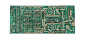
How do vias work in PCB prototypes?
The design and placement of vias are critical factors in the performance of a PCB prototype. Proper via placement ensures that the electrical signals are routed efficiently and without interference. It also minimizes the risk of signal degradation, especially in high-speed designs. If vias are placed too close to sensitive components or traces, they can cause signal delays or introduce unwanted capacitance or inductance. Therefore, careful consideration must be given to the size, placement, and type of via used in a PCB prototype. The use of larger vias, for instance, can reduce resistance, but they also require more space and can affect the overall density of the design.
The process of creating vias in a PCB prototype typically involves drilling small holes through the layers of the board. Once the holes are drilled, they are plated with copper, which forms the electrical connection between the layers. The plating process must be precise to ensure good conductivity and avoid defects such as incomplete connections or shorts. This process is typically followed by further steps, such as etching the copper traces and applying protective layers, to complete the PCB prototype.
In addition to providing electrical connections, vias in PCB prototypes can also impact the mechanical strength of the board. The process of drilling and plating vias can create stress points in the PCB, especially when using multiple layers or small vias in high-density designs. This requires careful design consideration to ensure the board’s mechanical integrity and prevent failure during use or assembly.
In conclusion, vias are integral to the functionality of PCB prototypes, enabling the transfer of electrical signals between different layers of the board. The selection and placement of vias impact the overall design, performance, and reliability of the PCB prototype. By choosing the appropriate type of via and ensuring precise manufacturing, designers can create efficient, high-performance PCB prototypes that meet the specific needs of their applications. Whether for simple, single-layer designs or complex, multi-layer circuits, vias are essential components for modern electronic systems.


